When learning about new hardware, there are always different angles to look at it. For the most part, manufacturers talking to the media will focus on the hardware aspects of the new shiny thing, about what it can do at a high level then go into a low level silicon architecture detail (sometimes). Anything on the software side comes through talks about how to write for the new shiny thing – this is why Intel has conferences such as IDF (Intel Developer Forum) to help explain how to use it. Interestingly there can always be information about the true operating nature of the device in a software talk, as opposed to a hardware talk.
As such, I attended a tutorial session here at SuperComputing15 on the MCDRAM (Multi-Channel DRAM) used in Intel’s 2nd generation Xeon Phi, code named Knights Landing (KNL). Specifically the talk focused on the analysis methods and tools, and it went into greater depth as to how the implementation works.
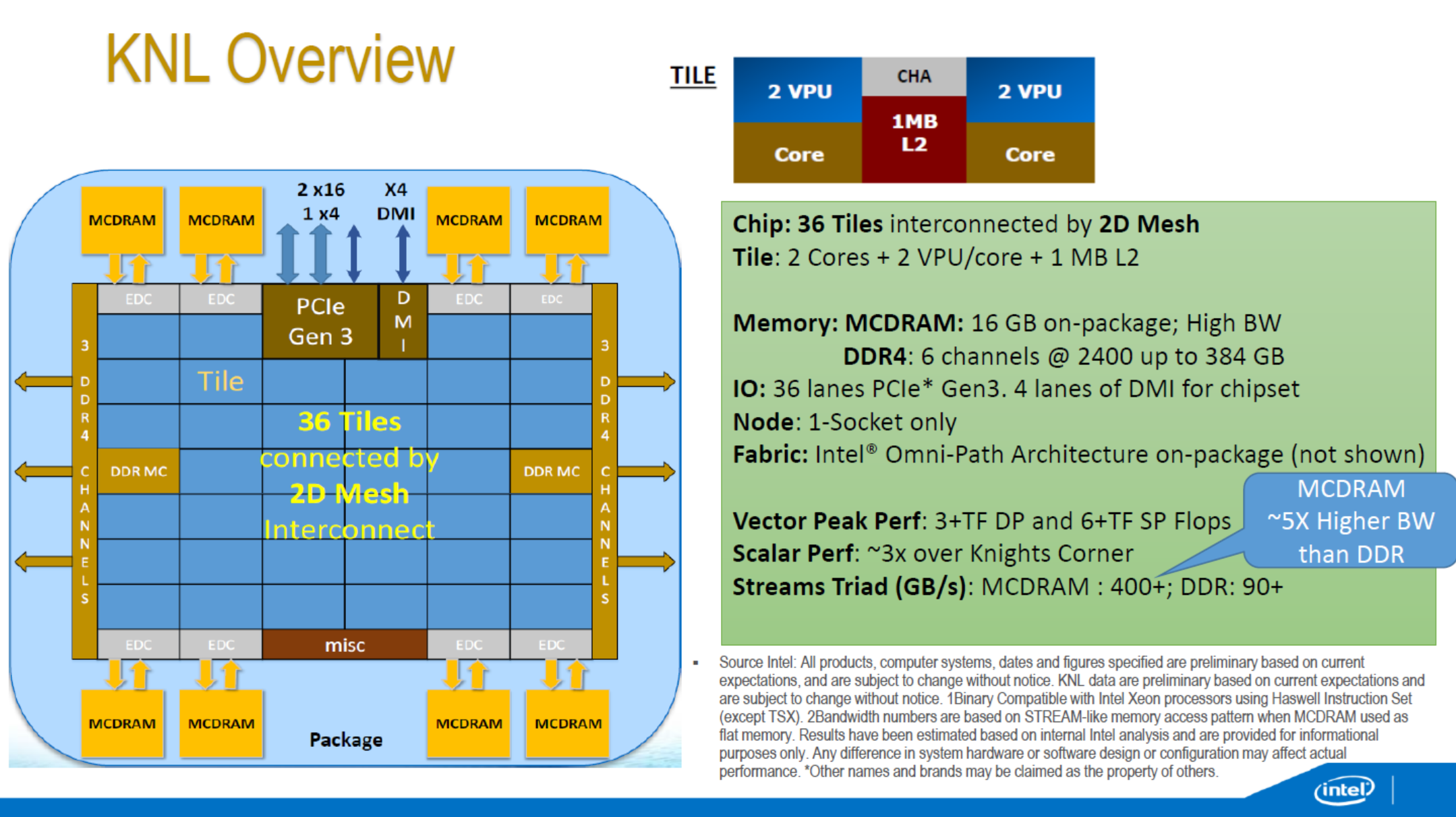
Some of the KNL overview we have seen before – the 72 Silvermont-based cores running at ~1.3 GHz are split into tiles with two cores per tile, two VPUs (Vector Processing Units, AVX-512) per core and each tile shares 1MB of L2 cache for a total of 36MB of L2 across the design. Rather than the ring topology we see in the standard processor designs from Intel, they are arranged in a mesh topology using an interconnected fabric (which seems to be sets of rings anyway). Despite the 6x7 nature of the image above, shots of the package have had some question that the layout is more akin to a 4x9, although this is unconfirmed.
The big paradigm shifts are everywhere. KNL can be used as the main processor in a computer, running an OS on top of all the cores, or as a co-processor similar to former Xeon Phi silicon – but as noted above in the slide there is no version of QPI for 2P/4P systems. There are a total of 36 PCI 3.0 lanes though, for PCIe co-processors, as well as onboard Omni-Path control for network interconnects. The cores are 14nm versions of Silvermont, rather than 22nm P54C, with claims that the out-of-order performance is vastly improved. The die has a total of 10 memory controllers – two for DDR4 controllers (supporting three channels each), and then eight for MCDRAM.
Each of these high-bandwidth controllers link out to a the on-package MCDRAM (we believe stacked 20nm Micron Planar DRAM) through an on-package interposer, offering 400+ GB/s of bandwidth when all the memory is used in parallel. This sounds similar to AMD’s Fiji platform, which offers 4GB of memory over four HBM (high bandwidth memory) packages, but Intel is prepared to offer 16GB of MCDRAM ‘at launch’. The fact that Intel says at launch could be suggested that there are plans to move into higher capacities in the future.
As the diagram stands, the MCDRAM and the regular DDR4 (up to six channels of 386GB of DDR4-2400) are wholly separate, indicating a bi-memory model. This stands at the heart at which developers will have to contend with, should they wish to extract performance from the part.
The KNL memory can work in three modes, which are determined by the BIOS at POST time and thus require a reboot to switch between them.
The first mode is a cache mode, where nothing is needed to be changed in the code. The OS will organize the data to use the MCDRAM first similar to an L3 cache, then the DDR4 as another level of memory. Intel was coy onto the nature of the cache (victim cache, writeback, cache coherency), but as it is used by default it might offer some performance benefit up to 16GB data sizes. The downside here is when the MCDRAM experiences a cache miss – because of the memory controllers the cache miss has to travel back into the die and then go search out into DDR for the relevant memory. This means that an MCDRAM cache miss is more expensive than a simple read out to DDR.
The second mode is ‘Flat Mode’, allowing the MCDRAM to have a physical addressable space which allows the programmer to migrate <a href="http://solucionariodatastructuresweiss.blogspot.com/"> data structures </a> in and out of the MCDRAM. This can be useful to keep large structures in DDR4 and smaller structures in MCDRAM. We were told that this mode can also be simulated by developers who do not have hardware in hand yet in a dual CPU Xeon system if each CPU is classified as a NUMA node, and Node 0 is pure CPU and Node 1 is for memory only. The downside of the flat mode means that the developer has to maintain and keep track of what data goes where, increasing software design and maintenance costs.
The final mode is a hybrid mode, giving a mix of the two.
No hay comentarios:
Publicar un comentario